 Swift Glass is a global leader in glass part fabrication with nearly 100 years of experience. We use an extensive selection of fabrication techniques to provide expertly crafted custom glass products. In addition to services such as chemical glass strengthening, thermal glass tempering, and drilling, we also fabricate glass carrier wafers for various technical applications.
Carrier wafers are a vital tool for microelectromechanical systems (MEMS) and the semiconductor industry. They act as a substrate for ultra-thin semiconductor wafers to be bonded to during fabrication, allowing for safe handling and processing while preventing damage. Carrier wafers are typically made from silicon or glass; however, glass offers many beneficial properties that may make it a superior choice.
How are Carrier Wafers Used?
As technology advances, devices are becoming smaller and smaller. Reducing the thickness of semiconductor wafers is essential to ensuring that the necessary chips and sensors can fit into the smallest spaces. Semiconductor wafers are fragile and flexible, meaning they require temporary stabilization to enable effective processing and to further decrease device wafer thickness. By temporarily bonding device wafers to carrier wafers, the device wafers can be carefully processed and handled without becoming damaged.
The thickness reduction process is known as thinning. This process begins by bonding a flipped device wafer to a carrier wafer. Then thinning and processing of the silicon wafer occurs, and finally, the two are de-bonded. While silicon wafers can be used as the carrier wafer during this process, they are not the only available option. Alternative materials, such as glass, can be used and provide several noteworthy advantages.
What Are Glass Carrier Wafers?
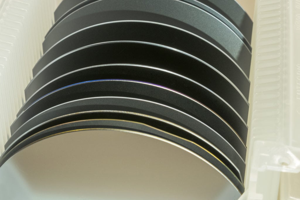
Glass carrier wafers are precision disks of thin glass, such as borosilicate glass. They are created by selecting an appropriate high-quality glass material and then carefully cutting and shaping it. Numerous finishing processes are performed to perfect the carrier wafer’s flatness before it undergoes rigorous quality inspection processes using precision laser measuring equipment.
Similar to silicon carrier wafers, glass carrier wafers are used as a bonded substrate in the fabrication process of thinner device wafers. Common applications for glass carrier wafers include:
- Electronics and MEMS. Glass carrier wafers are used as substrate carriers during the thinning process of silicon wafers for MEMS and various electronics.
- Semiconductors. Glass carrier wafers are used as a temporary bonding substrate for handling thin, flexible, and delicate semiconductor wafers.
- 3D-IC applications. Glass carrier wafers have proven to be beneficial during wafer thinning operations for three-dimensional stack IC structures.
Advantages of Glass Carrier Wafers Over Silicon Carrier Wafers

Although silicon carrier wafers are a popular choice, it’s important to note that glass carrier wafers offer many unique benefits that may make them the superior option. Specific advantages of glass carrier wafers include:
- Transparency. The transparency of glass carrier wafers aids in the debonding process and allows for in-process inspection. It also makes it easier to identify any bonding issues.
- Desirable properties. Glass is an excellent choice for carrier wafers due to its many desirable properties, including chemical resistance and mechanical strength. Glass also features good thermal stability, minimizing the risk of warping.
- Cost-effective and sustainable. Glass carrier wafers can be cleaned for reuse, contributing to cost savings and environmental protection.
- Durability. Glass carrier wafers offer excellent functionality and reliability over time, even when exposed to harsh environments.
- Form and shape. Glass is characterized by its smoothness and flatness, which makes it suitable for use as a carrier substrate. Glass carrier wafers also feature the same notch and edge bevel as silicon carrier wafers while exhibiting the additional benefits of glass.
Get Quality Glass Wafers From Swift Glass
Glass carrier wafers are used throughout several applications, such as MEMS, semiconductors, and more. In comparison to silicon, glass substrate carriers are flatter, stiffer, and provide superior thermal stability so that device wafers can be handled safely. In many situations, glass carrier wafers not only outperform silicon but are also more cost-effective.

