Category Archive: Glass Wafers
Micro-electromechanical systems (MEMS) combine mechanical and electrical capabilities into a single glass wafer. Nearly every industry has found a way to integrate these tiny devices into their production lines, including the automotive, semiconductor, medical, communications, and consumer electronics industries. In fact, the consumer electronics market is projected to grow about 8.6% annually, in large part thanks to the rise of MEMS technology.
Learn more about MEMS, why glass is the ideal substrate for them, and our fabrication capabilities.
What Are Micro-Electromechanical Systems (MEMs)?
MEMS are minuscule, powerful integrated devices or systems that combine electrical and mechanical components. MEMS fabrication involves integrated circuit (IC) batch processing techniques, using glass wafers as substrates. MEMS devices can detect, control, and actuate micro processes, creating effects on a macro scale. The final product ranges from a few millimeters to less an a micrometer in size, which is smaller than the width of a human hair.
“MEMS” was coined in a 1986 technical paper to the Defense Advanced Research Projects Agency (DARPA) and has since become the term that describes the fabrication of tiny electromechanical devices as well as the devices themselves. Fabrication of a MEMS may not include mechanical components, but they are still termed MEMS because of their size and structure. They are known in Europe as microsystem technology (MST) and in Japan as micromachines.
Uses of MEMs
From their humble beginnings in the early 1950s, MEMS have since journeyed from research labs to everyday consumer products. MEMS started appearing in commercial applications like airbags in cars, inkjet printers, and medical-grade pressure sensors in the mid-1990s. Today, these devices are even more ubiquitous—every new car contains at least 50 MEMS, for airbags as well as mandated safety systems, tire pressure monitoring systems, and electronic stability control.
Another example of MEMS that people use every day is the system on a chip (SOC) on smartphones that automatically changes screen orientation. As MEMS require less power, become smaller, and become less expensive to fabricate, these devices will play a key role in home automation and Internet of Things (IoT) ecosystems.
Common applications containing MEMS include:
- Heating and cooling systems in buildings driven by sensors
- High-definition projection using micromirror arrays
- Detecting subtle changes in cleanrooms and other nanotechnology manufacturing environments
- Inkjet printer micronozzles
- Mobile app integration of gyroscopes, accelerometers, barometers, and microphones
- Disposable medical pressure sensors
- Optical switching devices to control signals
Components of MEMS
MEMS contain mechanical microstructures, microactuators, microsensors, and microelectronics, integrated into a single chip. Microsensors sense changes in the device’s environment by monitoring thermal, chemical, mechanical, or electromagnetic information. Microelectronic components process this data and signal the microactuators to react to these changes.
The Rising Importance of Glass for MEMs
Silicon has long been the material of choice when fabricating MEMS, but researchers and manufacturers have identified alternative substrate materials that offer the same or more benefits than silicon. Some of these options include glass, quartz, metals, crystalline insulators, polymers, and ceramics.
In particular, the MEMS and electronics industries use glass as substrate carriers and in wafer packaging. Glass carrier substrates are preferable because of their chemical resistance and thermal stability. For medical device applications, glass wafers provide airtight MEMS enclosures. Glass wafer packaging offers greater functionality and reliability over time and in harsh operating conditions. Overall, glass is a desirable alternative to silicon for its lower cost, biocompatibility, and optical transparency.
Microfluidic devices also tend to use glass because of its chemical inertness and receptiveness to coatings. Four common applications of glass MEMS micromachining for microfluidics include:
- Flow cell and flow cell components
- Slides manufacturing
- Lab on a chip
- Bio-MEMS
MEMS glass fabrication is also popular for producing cost-effective, high-performance, and flexible microprocessors. As MEMS glass fabrication advances, so will the need to develop better micromachining methods. Traditional methods like CNC machining are ineffective on brittle glass materials. Fabrication methods must also adapt to the increasing diversity of MEMS applications, as features shrink in size and become more complex.
Learn More About Swift Glass’s Capabilities
Swift Glass has over 80 years of experience in glass design and fabrication, including MEMS glass wafers. Whether you need standard or custom-designed glass wafers, we use high-quality materials, advanced cutting and finishing tools, and a wealth of industry expertise. To learn more about glass wafers for the MEMS industry, download our eBook, “Glass Fabrication for MEMS Applications.” To begin your glass wafers for the MEMS industry fabrication project, contact Swift Glass or request a quote.
 Swift Glass is a global leader in glass part fabrication with nearly 100 years of experience. We use an extensive selection of fabrication techniques to provide expertly crafted custom glass products. In addition to services such as chemical glass strengthening, thermal glass tempering, and drilling, we also fabricate glass carrier wafers for various technical applications.
Carrier wafers are a vital tool for microelectromechanical systems (MEMS) and the semiconductor industry. They act as a substrate for ultra-thin semiconductor wafers to be bonded to during fabrication, allowing for safe handling and processing while preventing damage. Carrier wafers are typically made from silicon or glass; however, glass offers many beneficial properties that may make it a superior choice.
How are Carrier Wafers Used?
As technology advances, devices are becoming smaller and smaller. Reducing the thickness of semiconductor wafers is essential to ensuring that the necessary chips and sensors can fit into the smallest spaces. Semiconductor wafers are fragile and flexible, meaning they require temporary stabilization to enable effective processing and to further decrease device wafer thickness. By temporarily bonding device wafers to carrier wafers, the device wafers can be carefully processed and handled without becoming damaged.
The thickness reduction process is known as thinning. This process begins by bonding a flipped device wafer to a carrier wafer. Then thinning and processing of the silicon wafer occurs, and finally, the two are de-bonded. While silicon wafers can be used as the carrier wafer during this process, they are not the only available option. Alternative materials, such as glass, can be used and provide several noteworthy advantages.
What Are Glass Carrier Wafers?
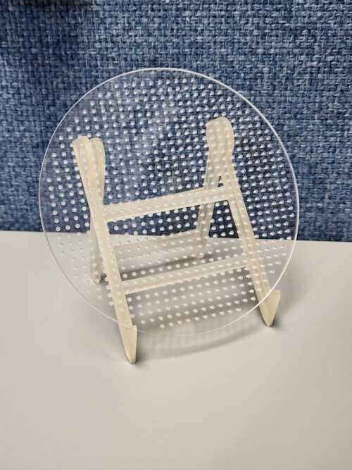
Glass carrier wafers are precision disks of thin glass, such as borosilicate glass. They are created by selecting an appropriate high-quality glass material and then carefully cutting and shaping it. Numerous finishing processes are performed to perfect the carrier wafer’s flatness before it undergoes rigorous quality inspection processes using precision laser measuring equipment.
Similar to silicon carrier wafers, glass carrier wafers are used as a bonded substrate in the fabrication process of thinner device wafers. Common applications for glass carrier wafers include:
- Electronics and MEMS. Glass carrier wafers are used as substrate carriers during the thinning process of silicon wafers for MEMS and various electronics.
- Semiconductors. Glass carrier wafers are used as a temporary bonding substrate for handling thin, flexible, and delicate semiconductor wafers.
- 3D-IC applications. Glass carrier wafers have proven to be beneficial during wafer thinning operations for three-dimensional stack IC structures.
Advantages of Glass Carrier Wafers Over Silicon Carrier Wafers

Click to Enlarge
Although silicon carrier wafers are a popular choice, it’s important to note that glass carrier wafers offer many unique benefits that may make them the superior option. Specific advantages of glass carrier wafers include:
- Transparency. The transparency of glass carrier wafers aids in the debonding process and allows for in-process inspection. It also makes it easier to identify any bonding issues.
- Desirable properties. Glass is an excellent choice for carrier wafers due to its many desirable properties, including chemical resistance and mechanical strength. Glass also features good thermal stability, minimizing the risk of warping.
- Cost-effective and sustainable. Glass carrier wafers can be cleaned for reuse, contributing to cost savings and environmental protection.
- Durability. Glass carrier wafers offer excellent functionality and reliability over time, even when exposed to harsh environments.
- Form and shape. Glass is characterized by its smoothness and flatness, which makes it suitable for use as a carrier substrate. Glass carrier wafers also feature the same notch and edge bevel as silicon carrier wafers while exhibiting the additional benefits of glass.
Get Quality Glass Wafers From Swift Glass
Glass carrier wafers are used throughout several applications, such as MEMS, semiconductors, and more. In comparison to silicon, glass substrate carriers are flatter, stiffer, and provide superior thermal stability so that device wafers can be handled safely. In many situations, glass carrier wafers not only outperform silicon but are also more cost-effective.
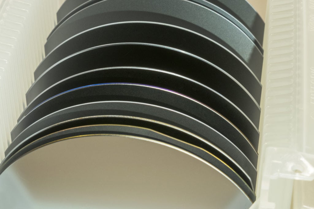
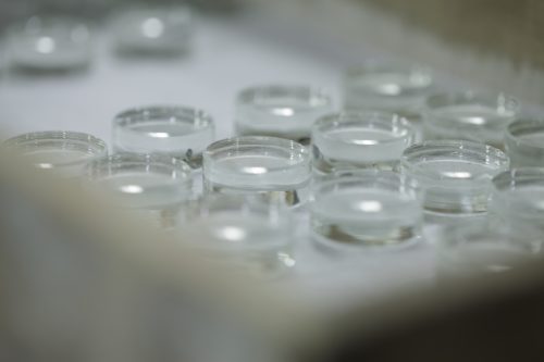
Glass wafers are thin, circular precision glass pieces, typically made from quartz, borosilicate glass, or fused silica. They are a necessary component for a variety of common electronics, such as electronic screen and display assemblies, and see use throughout a variety of industrial applications as well.
Swift Glass has nearly 100 years of experience delivering expertly fabricated glass parts. We employ the latest innovations in glass fabrication technology in conjunction with the highest-quality materials, enabling us to deliver reliable glass wafers. Read on to learn more about the glass wafer fabrication process, as well as the latest wafer trends.
The Glass Wafer Fabrication Process
click to expand

At Swift Glass, our experts craft glass wafers that meet even the most challenging design requirements. The fabrication process involves five steps:
- Selecting Materials: Depending on each customer’s design requirements, an appropriate high-quality glass is selected. We work with borosilicate (including Borofloat®), quartz and fused silica. Borosilicate is highly affordable and retains excellent mechanical strength in challenging environments. Quartz is shock-resistant and features a high melting point.
- Cutting and shaping: After the materials have been selected, the cutting process begins. Using our advanced portfolio of glass machining equipment, we can cut orders up to 100,000 wafers.
- Edging and Detailing: Next, the glass wafers are further refined through edge grinding and detailing processes. The fabrication process uses carefully calibrated CNC diamond machine tools and each wafer is delicately machined to design specifications.
- Lapping and Polishing: We use a free abrasive lapping process to develop appropriate surface smoothness before polishing each wafer on both sides.
- Inspection: Wafers undergo a high precision laser inspection in a clean room to ensure that they fall within total thickness variation (TTV) standards.
Wafer Fabrication Trends & Challenges
Change and innovation in technology are constantly occurring. In wafer fabrication, the demand for thinner wafers has been increasing, causing manufacturers to adapt to the challenges this presents. Thinner wafers have edges that are more susceptible to chipping. This makes edge finishing processes to improve edge protection and decrease the likelihood of chipping necessary.
Using silicon materials has become another trend in wafer fabrication. Silicon has excellent thermal properties and can be more cost-effective than glass. However, glass wafers have certain unique advantages over silicon. For example, its transparency makes discovering any bonding defects much easier. Additionally, some temporary bonding polymers require transparent substrates, making glass the preferred material for these applications.
Many customers need to customize their glass wafers with finishes that include channels, cavities, or holes on the wafer surface. Swift Glass leverages value-added processes like ultrasonic machining and microblast machining to target highly precise areas of delicate parts. Ultrasonic machining removes small amounts of glass using high-frequency vibrations, without compromising the glass’s chemical or physical structure. Microblast machining can target substrates on a microscopic level to etch glass surfaces.
Glass Wafer Fabrication From Swift Glass
Swift Glass offers fully customized glass wafer fabrication for everything from prototypes to high-volume production runs. As an ISO 9001:2015- and ITAR-certified company, we use high-quality, reliable materials and the most advanced equipment available for each step of the fabricThis blog post discusses the glass wafer fabrication process and the latest trends in glass wafer fabrication.ation process.
Our capabilities include CNC machining, ultrasonic machining, microblast machining, thermal tempering, chemical strengthening, and more. For more information about our glass wafer fabrication capabilities at Swift Glass and how they will benefit your application, please contact us or request a quote today.
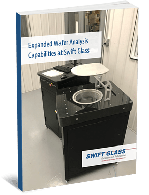
Glass wafers have a variety of applications throughout the electronics, computer, and biotechnical manufacturing fields. During production, the ability to make precise measurements ensures that wafers fit the necessary specifications for their intended purpose. A Multi-Surface Profiler (MSP) machine supports high-precision metrology in the production of glass wafers for industrial purposes.
With the addition of the Tropel® FlatMaster® MSP-300 Machine to our operations, Swift Glass is now able to provide high-speed, incredibly precise metrology for 300 mm glass wafers.
Wafer Measurement Capabilities
The Tropel® FlatMaster® MSP-300 is a high-frequency stepping interferometer that gives our team new capabilities. Using this MSP machine, our technicians can collect over 3 million data points with accurate measurements at the submicron level—all in a matter of seconds. Wafer thickness and flatness characterizations across the wafer’s entire surface can be measured with high precision.
Capabilities at Swift Glass
With the Tropel® FlatMaster® MSP-300 bolstering our fleet of state-of-the-art equipment, the team at Swift Glass has added important capabilities to our arsenal of advanced services. In addition to interferometrics and other glass wafer services, our capabilities include:
- CNC machining
- Surface lapping
- Glass drilling
- Thermal glass tempering
- Waterjet and glass cutting
- Chemical glass strengthening
- Surface polishing
- Edge polishing and grinding
The addition of the Tropel® FlatMaster® MSP-300 demonstrates our commitment to continuous improvement and our willingness to invest in the latest glass fabrication practices, ensuring we produce custom glass wafers that meet the specifications of our clients.
Contact Swift Glass to learn how our new capabilities can support your next project. Learn more about our expanded wafer analysis capabilities in our guide below.